| |
|
|
| |
|
 |
 |
|
 |
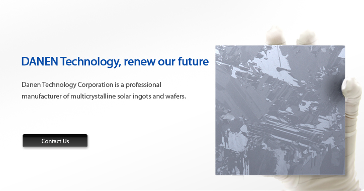
| Danen produces multi solar wafers, from which the solar cell conversion efficiency reaches above 17.6% in average, and customers can produce 18% efficiency solar cells through our ultra-high efficiency wafers ; we own ultra-thin slicing technology for wafers with 160~180μm thickness, the company also filed patents of specialized crystallization technology. Major customers are tier one solar cell makers located in Taiwan, Europe, and Asia. Besides selling our own wafers, DANEN also provides customized OEM service, we are one of the leading high efficiency multi-crystalline wafer manufacturers in Taiwan. Understand more about our R&D technology |

 |
| Danen’s production site is based in Guanyin, Taoyuan County. The solar cell conversion efficiency reaches above 17.6% in average, and customers can produce 18% efficiency solar cells through our ultra-high efficiency wafers.
The capacity of wafer plant I is 120MW in
2010, and the wafer plant II of 210MW
capacity was already completed in Q2, 2011;
plus the wafer plant III which is under
construction, the total capacity will reach
550MW. ….....Understand more about our R&D technology |
 |
| Note: |
1.This specification is subject to update without notice. |
|
2.Contact our sales representative for detail information. |
|
 |
| Physical |
| Crystalline |
Multi-Crystalline |
|
| Electrical |
| Resistivity |
0.5~3.0 Ohm-cm |
|
| Mechanical |
| Dimension |
156 ± 0.5 * 156 ± 0.5mm |
| Average Wafer Thickness |
Nominal thickness ± 10% (200 um or 180 um) |
|
|
|
|
|
|
|